Detailed knowledge of solar photovoltaic technology (2)
Detailed knowledge of solar photovoltaic technology (2) (1)

Manufacturing process of crystalline silicon solar cells
The manufacturing process of crystalline silicon solar cells is described as follows:
(1) Slicing: Using a multi-wire cut, the silicon rod is cut into square silicon wafers.
(2) Cleaning: It is cleaned by a conventional silicon wafer cleaning method, and then the surface of the silicon wafer is cut with an acid (or bismuth) solution to remove the damaged layer by 30-50 um.
(3) Preparation of suede: Anisotropic etching of the silicon wafer with a bismuth solution was carried out to prepare a suede surface on the surface of the silicon wafer.
(4) Phosphorus diffusion: The coating source (or liquid source, or solid phosphorus nitride sheet source) is used for diffusion to form a PN+ junction, and the junction depth is generally 0.3-0.5 um.
(5) Peripheral etching: A diffusion layer formed on the peripheral surface of the silicon wafer during diffusion causes short-circuiting of the upper and lower electrodes of the battery, and the peripheral diffusion layer is removed by masking wet etching or plasma dry etching.
(6) Remove the back PN+ junction. The back side PN+ junction is removed by conventional wet etching or grinding.
(7) Production of upper and lower electrodes: a process such as vacuum evaporation, electroless nickel plating or aluminum paste printing and sintering. Make the lower electrode first, then make the upper electrode. Aluminum paste printing is a widely used process.
(8) Making an anti-reflection film: In order to reduce the reflection loss, an anti-reflection film is coated on the surface of the silicon wafer. The materials for making the anti-reflection film are MgF2, SiO2, Al2O3, SiO, Si3N4, TiO2, Ta2O5 and the like. The method may be a vacuum coating method, an ion plating method, a sputtering method, a printing method, a PECVD method, or a spray method.
(9) Sintering: The battery chip was sintered on a bottom plate of nickel or copper.
(10) Test binning: Test classification according to the specified parameter specifications.
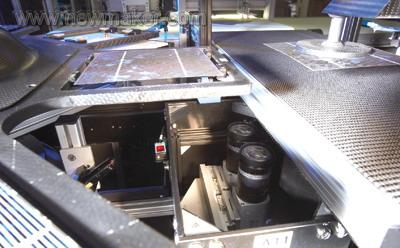
It can be seen that the manufacturing method of the solar cell chip is basically the same as that of the semiconductor device, and the production process equipment is basically the same, but the processing precision is far lower than the manufacturing requirement of the integrated circuit chip, which provides for the scale production of the solar cell. Favorable conditions.
Kylin Chemicals manfacturers & supplies high performance flocation flocculants & collectors, serving the various mining industries like coal, phosphorous, copper, lead, nickle, gold, silver, potassium & sand-washing, etc. Our advanced manufacturing facilities and effective quality control systems, ensures every delivery of goods fully meets/exceeds our customers` end using needs. Today, our flocation flocculants & collectors have been widely accepted by various mining industries in Southeast Asia, Middle East and Latin America.


Flotation Flocculants & Collectors
Flotation Flocculants & Collectors,Potassium Amyl Xanthate,90% Potassium Amyl Xanthate,Industrial Potassium Amyl Xanthate
Kylin Chemicals Co., Ltd. , http://www.kylin-chemicals.com