In the "technical application" of single crystal, polycrystalline silicon wafer production process detailed (above), the author introduced the first half of the monocrystalline and polycrystalline silicon wafer process flow, outlines some of the process flow and concepts, as well as related knowledge of terms. This article starts with the slicing process, grinding and gettering, and seeing how silicon changes.
slice
Slice review
When the single crystal silicon rod is sent to the silicon wafer production area, the crystal rod has passed the process of head and tail cutting, barrel grinding, and reference surface grinding. The carbon plate is directly bonded, and bonding with the dicing block can be performed. .
To be able to cut a single silicon wafer, the crystal rod must be cut in some way. The slicing process has some requirements: it can be cut in a specific direction of the crystal; the cut surface is as flat as possible; the damage introduced into the silicon wafer is as small as possible; and the material loss is as small as possible.
Carbon plate
When the silicon wafer is cut from the boule, something is needed to prevent the wafer from falling loose. Typically, the carbon plate and the crystal rod are bonded together by epoxy so that the silicon chip is stuck on the carbon plate after being cut from the crystal rod.
Carbon plates are not the only choice for adhesive plates. Any kind of adhesive plate and epoxy bonding agent must have the following characteristics: It can support the silicon chip, prevent it from falling during the slicing process and can be easily removed from the adhesive plate and Epoxy on the peel; also protect the silicon from contamination. Other adhesive board materials include ceramics and epoxy.
Figure 2.1 illustrates the bonding of a carbon plate to a crystal rod.
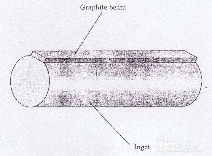
Figure 2.1 sticky stick schematic
graphite
It is a hard material used to support the silicon wafer. It is made into the same shape as the bonding area of ​​the crystal rod. In most cases, carbon plates should be adhered strictly along the reference surface of the crystal rod so that the carbon plate can be processed into rectangular strips. Of course, the carbon plate can also be bonded to other parts of the crystal rod, but it should also conform to the shape of the part. The shape of the carbon plate is important because it requires the use of as little epoxy as possible and the shortest possible distance between the carbon plate and the crystal rod. This distance requirement is as short as possible because epoxy is a rather soft material and carbon and crystal rods are very hard materials. When the blade is cut from a hard material to a soft material to a hard material, it can cause the silicon chip to crack.
Here are some options for selecting epoxy types: strength, mobility and degree of contamination. Epoxy bonding carbon plate and crystal rod should have sufficient viscosity to support the wafer until the entire crystal rod is cut. Therefore, it must be easily removed from the wafer with only a minimal amount of contamination.
blade
When cutting the silicon wafer from the ingot, it is desirable that the cut surface is flat, the damage is small, the material cut in a specific direction and the material lost is as small as possible. It is worthwhile to have a fast, safe, reliable and economical cutting method.
In semiconductor companies, two commonly used methods are ring cutting and wire cutting. Ring cutting usually refers to internal circle cutting, and is the most widely used method for cutting crystal rods into silicon wafers.
Inner circle cutting
The inner circle is cut and the cutting position is on the surface of the blade. The blade is a large, thin ring made of stainless steel. The inner edge of the blade is plated with a layer of nickel with diamond particles. This diamond-nickel coating provides the surface for cutting the crystal rod. For a 150mm wafer, it takes 3 minutes per tool.
Inner blade composition and thickness
For a typical inner blade, the center portion is made of about 0.005 inch stainless steel, and the nickel-diamond coating is about 0.003 inch on both sides of the stainless steel blade edge. The inner edge of the inner blade has a total thickness of about 0.0125 inches. In this way, the material loss thickness is slightly greater than the maximum thickness of the blade, which is approximately 0.013 inches.
The thickness of the nickel-diamond coating is an important parameter for the inner circular insert. Obviously, the smaller the thickness, the less blade loss. However, if the coating is too thin, the path cut by the blade is too narrow, the blade may have more potential potential impact edges, if any deviation of the blade hits the edge, the wafer will be damaged in the next step Need to remove more material. Therefore, there is an optimum nickel-diamond coating that can achieve the lowest material loss.
The high ductility of stainless steel allows the blade to have a great tension. This strong tension allows the blade to stretch very tightly, keeping the blade flat during cutting. Another advantage is that it is very durable and can be used with the same blade without replacement, thus reducing the production costs of the silicon wafer. This is important because replacing a blade takes about 1.5 hours.
For the same size of crystal rod, there is a way to reduce the size of the blade, that is, round the crystal rod before cutting. The advantage of this arrangement is that it does not require such a large diameter as long as it passes half the path of the crystal rod when slicing the inner circle. However, it can lead to chipping and defects in the center of the wafer. As the diameter of the crystal rod increases, the inner circle slices become less practical.
Slice damage
When the microtome is cutting a crystal rod, it can cause a lot of damage. This process can cause many fine cracks and cracks in the silicon wafer. The average thickness of this damaged layer is about 25-30 μm. Such damage exists anywhere the blade comes in contact with the crystal stick. Because the chips touch the surface of the silicon wafer, there are many such damages on the surface of the silicon wafer. This means that these damages must be removed in the next process before the silicon wafer can be useful.
Blade deflection
The main source of wafer bending and thickness deviation is in the slicing process. The most important factor affecting the shape of the wafer is the blade deflection during the slicing process. If the blade vibrates during slicing, it is very likely that the damage layer on the blade side will be deeper than on the other side. The difference is that the damage caused by blade vibration is called slice differential damage.
Fragments (when blade exits)
In any way, when the blade cuts a certain material to be completed, the blade may cause the material to crack when it is at the bottom of the material. This phenomenon is called an exit chip. The occurrence of debris is due to the presence of high local stresses in small areas of the material during the final stages of cutting. When continuously applying the same amount of pressure on increasingly thin materials, the material can no longer withstand such pressure. This piece of material begins to break and pieces of material loosen.
Minimal (fragmentation)
There are two ways to prevent the occurrence of debris. One method is to reduce the pressure applied to the wafer by the blade in the final stage. In the end, the pressure can be reduced by lowering the blade feed rate. Another method is to attach a few pieces of material to the outside of the crystal rod to complete the cutting. The addition of additional material to the outer surface provides a carrier that facilitates the completion of the slicing. This reduces the pressure on the thinner edges of the silicon wafer and does not break the silicon wafer.
There is a system to prevent fragmentation that can eliminate the occurrence of any debris. It is to make the diameter of the crystal rod slightly larger, then there is still enough material at the time of slicing, even if debris occurs, and it is barreled to the cracked place. The application of this method makes the crystal rod diameter about 1.3mm. After slicing, excess material is removed.
In addition to the inner circle cutting, there is a line cutting.
Wire cutting uses a grout to cut a crystal rod. The mortar is attached to a steel wire that comes into contact with and enters the crystal rod. The steel wire generates pressure and pressurizes the abrasive and the crystal rod, so that the pressure contact between the mortar and the crystal rod makes the material be Grind away.
The basic structure of wire cutting is very simple. A small diameter steel wire is wound around several guide wheels to form a trapezoidal shape of the wire. Grooves in the guide wheel ensure that the steel wires are separated by a certain distance. A continuous steel wire is concentrated around one groove of the guide wheel, forming many equally spaced cutting surfaces. The space between the lines determines the desired thickness of the wafer. The movement of the steel wire is controlled by a spool. The entire system has only one steel wire. Both ends of the wire are wound around the spool, and the crystal rod moves slowly upwards (downwards) through the steel wire. The steel wire can cut many silicon wafers from the crystal rod at the same time. Such as 150mm silicon wafer, the entire crystal rod cutting is completed only about 5-8 hours.
A typical wire cutter uses a wire diameter of about 0.006 inches. The slicing loss caused by such a small size is only 0.008 inches. The single line is usually 100 km long and is wound on two spools. The application of such a long steel wire makes it impossible for a single area of ​​the wire to come in contact with the mortar and the crystal rod for a long time. This reduction in contact time with the mortar helps to extend the life of the steel wire. A typical wire feed rate is 10 m/s (22 mph), ie a 100 km long steel wire takes 10,000 seconds or about 2.75 hours in one direction. One of the wire guide wheels is driven by a motor to control the entire wire system.
The steel wire must maintain a certain tension to oppress the frosted grinding crystal rods in the mortar and prevent the steel wire feeding error on the guide wheels.
The steel wire of the wire cutter is in contact with the crystal rod, and the mortar is deposited on the steel wire. The mortar is a mixture of silicon carbide and oil, or some other similar mixture of hard material and liquid. Driven by the steel wire, the mortar slowly grinds the crystal rod and takes a little material on the surface of the crystal rod to form a groove. The constant movement of the steel wire continuously takes away the material in the groove. After the steel wire completely passes through the crystal rod, the mortar still moves along with the steel wire.
Wire cutting problem
There are two main types of failure modes: erroneous changes in wire tension and wire breaks. If the tension of the steel wire is wrong, the wire cutting machine cannot cut effectively. Any loosening of the steel wire will cause it to sway during cutting of the crystal rod, causing cutting losses and damage to the silicon wafer. Another problem occurs with low tension, which can cause erroneous feeding of the wire guide pulley. This error may cause erroneous cutting of the crystal rod or break the steel wire. During the cutting process, the steel wire may jump from one groove to another, cutting the wafer halfway. The steel wire may also be too tensioned to reach the limit it can withstand, causing the wire to break. If the wire breaks, it may damage the wafer and stop the cutting process. Broken steel wire may also cause the fracture of many silicon wafers.
Crystal orientation
When cutting, it must be cut in one direction according to customer requirements. All customers want the silicon wafer to have a specific crystal orientation, whether in a single crystal plane or if there is a specific, plane-specific orientation. It is necessary to make the cutting of the silicon chip as close as possible to this direction. Some fabrication processes rely on crystal etching, while others require the crystal orientation of the base layer to be accurate. Any problems with the orientation of the silicon wafer can cause device fabrication problems. Therefore, the correct orientation of the wafer must be checked at the beginning of the slicing.
When the stick is stuck on the microtome, the crystal rod is lined up on the reference plane. However, there is no guarantee that the crystal orientation of the cut wafer will be correct unless two silicon wafers are cut first and the crystal orientation is checked with an X-ray machine. If the crystal orientation of the wafer is incorrect, then the position of the crystal rod on the microtome must be adjusted. The slicer has the function of adjusting the crystal orientation.
Carbon plate removal
After the slicing is completed, the carbon plate stuck to the silicon wafer needs to be removed. The epoxy that bonds the silicon wafer to the carbon plate can be easily removed. Care should be taken when handling so that the edge of the wafer does not chip and keep the wafer in the same order.
The original order of the wafer must be maintained until laser engraving.
Laser lettering
After slicing and cleaning, the silicon wafer must be engraved with a laser mark.
The laser marking is generally engraved on the front edge of the silicon wafer and the laser evaporates the silicon to form the marking. The logo can be Greek letters or bar codes. Bar codes have an advantage because the machine can read it quickly and easily, but it is hard to read.
Because the laser marks are on the front side of the wafer, they may be wiped off during wafer production unless the engraved depth is deep enough. However, if it is too deep, it may be contaminated in the later process. General laser engraving depth is about 175μm.
What is usually done in the laser-engraved area is another task that is based on the physical properties of the silicon wafers, usually classified by thickness. The reason for non-conformity is usually due to chipping, breakage, warpage or excessive thickness.
Edge chamfering
Chamfers give the silicon edge a sleek profile. The main purpose of this operation is to eliminate the stress at the edge of the wafer during slicing. An additional benefit of edge chamfering is the ability to clear some small pieces of debris during the slicing process.
Edge chamfer pattern
The shape of the silicon edge is determined by the shape of the grinding wheel. The chamfer grinding wheel has a bullet-type grinding groove.
The outline of the edge of the silicon wafer is first completed by a vacuum suction head that sucks and rotates the silicon wafer. The silicon wafer slowly rotates, and the grinding wheel rotates at a high speed and presses against the edge of the wafer with a certain force. This system of moving the chamfer grinding wheel along the edge shape of the silicon wafer maintains the contact of the grinding wheel with the edge of the silicon wafer. This allows the reference surface to also be chamfered by the grinding wheel. After the wafer is rotated a few times, the edge of the wafer can get the shape of the grinding wheel groove.
Since the reference surface of the wafer is also chamfered at the same time, there are some problems. One problem is that when the reference surface is chamfered, it may be worn away. Because the reference plane is used for wafer alignment in some processes, this reference needs to be maintained.
Chamfer grinding wheel
The chamfer grinding wheel is a metal disc that is used to chamfer edges and is about 2-4 inches in diameter. The grinding wheel is about 0.25 inches thick and has a bullet-type groove at the edge of the disc. The grinding surface of the grinding wheel is a nickel-drilled coating.
Chamfering reason
A common factor in chamfering is that such edges can result in higher yields for both wafer production and device fabrication.
Break and break
When wafer edge chamfering is performed, high stress points at the wafer edge are removed. The drop in stress at the edge of the silicon wafer gives the silicon wafer higher mechanical strength. This helps to have greater resistance to chipping when handling wafers.
Outer edge crown crown
When epitaxy is grown on a silicon wafer, the epitaxial layer grows faster in areas with fine particle protrusion and high stress. Since these two conditions exist on the edge of the wafer before the chamfering is performed, the epitaxial layer tends to grow faster at the edges. This leads to small bulges on the edge of the silicon wafer. This bulge is called an epi-rim top and may cause problems in later device fabrication. If the edges of the silicon wafer have been chamfered, no high stress points or particle protrusions will make the epitaxial layer grow at the edges, which is conducive to the prevention of the formation of epitaxy crown crowns.
Edge photoresist beads
When a photoresist is applied to a silicon wafer, it is applied to a rotating silicon wafer. After applying a resist on the silicon wafer, the rotation speed will increase, so that the resist on the wafer will be thrown out and formed uniformly. Film. The problem is that due to the tension on the surface of the photoresist, beads will form at the sharp edges of the silicon wafer. If the wafer is not chamfered, the beads will stick to the surface of the wafer; if it has been chamfered, the beads will not form on the surface of the wafer.
Glossary
Slice microdamage (slice trace): caused by the vibration of the blade. During the slicing process, due to the small vibration of the blade, such damage was caused, leaving small ridge marks in the direction along the cut.
Slice loss: The total amount of material lost due to the blade during the slicing process.
Tension: It is used to describe the stretching ability of a material under load. In arithmetic terms, it is the degree of change in length compared to the original length.
Stress: refers to the force per unit area of ​​the material.
Swarf: Swarf refers to the material that is cut when the section is grooved. It can be considered as slice rubbish.
Tensile strength: refers to the maximum pressure that a material can withstand without complete failure.
Yield point: The maximum pressure a material can withstand without permanent deformation.
Grinding, heat treatment and related processes
After slicing, marking, and chamfering, it should be ready for polishing. Before the wafer can be polished, the chip damage must be removed. Next, the wafer needs to be etched to remove the damage caused by the wafer. The gettering process can offset the effects of metal impurities. Polishing on the edge of the silicon wafer removes the etch pit left on the edge of the wafer. The silicon wafer is then cleaned and heat treated and then annealed to stabilize the resistance. The backsealing process can be used at will, by depositing on the back side of heavily doped silicon wafers to prevent the dopants, usually boron, from escaping during the subsequent heat treatment. After the above steps, the silicon wafer can be polished.
Grinding
It is the use of abrasive sand to remove the material on the surface of the wafer and the damage left by the previous step. During the grinding process, both sides of the wafer are simultaneously ground in a double-sided planetary motion, and a certain amount of material will be ground away from both sides. This mechanical grinding process rubs off both sides of the wafer.
purpose
The main purpose of the wafer is to remove micro-damage from the silicon wafer. Slicing microdamage is the damage to the single crystal and comes from the slicing process. This damage is on both sides of the wafer because both sides of the wafer have been cut. The average depth of damage is about 25-30 μm, but some damage may be 2-3 times deeper.
The composition of the grinding disc
Grinding discs are generally made of cast iron but may also be made of plastic. Regardless of the contamination of the metal, the use of cast iron can be durable and its mechanical properties can be suitable for grinding. The hardness of cast iron makes the abrasive particles not embedded in the disk. If the particles are embedded in the grinding disk, the surface of the silicon wafer will be scratched. These scratches are difficult to remove in later processes, and the cast iron discs cannot be too hard. If the discs are too hard, they will force the abrasive particles into the wafer, adding extra damage to the wafer.
Grinding disc surface and grinding fluid supply
The grinding disc is geared, the gears facilitate the even distribution of the grinding liquid, prevent the grinding disc from being submerged, and keep the silicon wafer close to the surface. The gears also allow the fluid to flow across the surface of the wafer and distribute it evenly. If there is no gear on the disc, the abrasive may flow to the disc. If there is too much fluid between the disc and the wafer, the disc floats on the surface of the wafer. If the inner surface of the disc floats too far, the surface cannot be ground and the damage on the surface of the wafer cannot be removed. If there is too little grinding liquid between the grinding disc and the silicon wafer, the disc will cause new damage on the surface of the silicon wafer. Therefore, the gear controls the amount of grinding liquid between the grinding disc and the surface of the silicon wafer, and the gear of the upper grinding disc can lock the lower grinding disc. This prevents the silicon wafer from sticking to the upper grinding disc when the disc is finally separated.
Disc rotation counter
The upper and lower discs rotate in opposite directions. The rotation of the disc drives the wafers to rotate at the same speed on both sides. Objectives: First of all, since both sides of the wafer are polished at the same speed, both sides have the same material removal rate. Second, the opposite rotational speeds on both sides of the wafer allow the silicon wafer to be fixed. So there is no big pressure to move the wafer in one direction or the other. Silicon wafers hardly break due to the pressure of the edges.
The upper grinding wheel also has several functions. The first is that it has holes to allow the grinding fluid to flow into the grinding machine. The slurry flows from the upper plate and then flows into the machine. Another function is to provide pressure on the silicon wafer on the upper disc, the upper disc is pressed down by the pressure, in the first cycle of the disc, the pressure is relatively small, so that the high point on the wafer is first polished, so that the mill The liquid is evenly distributed inside the machine. Then, the pressure gradually rises to normal operating pressure.
Wafer thickness
In order to control the thickness of the grinding plate more precisely, a thickness testing system is installed on the grinding machine.
One way to test the thickness of a silicon wafer while polishing it is to use a piezoelectric material to grind it simultaneously with the silicon wafer. Because the piezoelectric material has the same abrasive rate as the silicon wafer, the frequency of the electrical signal changes. When the frequency corresponds to the set thickness, the machine will stop, but after each grinding, the piezo strip must be put back to the original, so as to reflect the thickness of the silicon wafer.
Silicon wafer surface removal
The surface of the wafer is ground using a grinding liquid consisting of a suspension of abrasive sand. Typical abrasive sands consist of 9 μm-sized calcined alumina particles. The particles are suspended in a mixture of water and additives. The additive is generally glycerol. The liquid mixture helps to keep the abrasive sand suspended and evenly spread.
The abrasive sand in the suspension presses the surface of the silicon wafer and wears it, removing the material on the surface of the wafer, which can remove the damage of the surface layer. The entire process grinds off the 75-100 μm surface. At the end of the final wafer, the flatness of the wafer is the flattest, and subsequent steps will reduce its flatness.
After grinding, there are many particles of silicon produced during the grinding process on the surface of the silicon wafer. This particle size is small and causes some problems. If you want to dry the wafer, the particles will stick to the surface of the wafer, and once it sticks, it will be difficult to remove. Therefore, the silicon wafer must remain wet until the surface particles are removed.
Stress release corrosion
After the silicon wafer has been polished, there is still a thin layer of damage, and other methods need to be used to remove the damage caused by the wafer. This damage is usually removed by chemically etching the surface of the silicon wafer. There are two methods of corrosion: alkali corrosion and acid corrosion.
When the silicon wafer is etched, it needs a clean surface. If the silicon surface is contaminated, it can potentially act as a mask for corrosion. When the acid is etched, the acid first comes into contact with the particles on the surface and slowly removes it, so that it is like a mask that affects the rapid contact of acid with silicon. This will cause the area to be inconsistently corroded with other areas of the wafer surface. Therefore, the silicon wafer must be cleaned before it is etched. A typical cleaning method is to place the silicon wafer in a cassette of Teflon and immerse it in a solution containing H2SO4 and hydrogen peroxide. This will remove the organic matter on the surface of the wafer; then the silicon wafer is immersed in hydrofluoric acid, and HF will remove any surface The end of the silicon; After the silicon wafer is cleaned, it can be etched and it will corrode evenly.
Alkali corrosion
One method of etching silicon wafers is to use alkaline hydroxides such as potassium hydroxide (KOH). In this way, the silicon wafer is immersed in a solution of 45% KOH and 55% pure water for about 2 minutes, usually in a high temperature (about 100°C) KOH solution. Then, the silicon wafer was immersed in pure water to block the continued reaction between KOH and the surface of the silicon wafer.
The basic reaction between KOH and silicon is as follows:
Si + 2H2O + 2KOH → 2H2 + Si(OH)2(O)2 + 2K+
Acid corrosion
Typical mixtures for acid etching are HNO3 and HF. In any case, acid corrosion is a strong process and there is no self-limiting process in a plane. The local corrosion rate of the acid bath can vary due to the loss of local chemicals. Because the silicon wafers are competing for acid around them, there is a tendency for the center of the silicon wafer to have insufficient etchants, which can cause loss of acid in the center of the silicon wafer and the response is slightly reduced. On the other hand, near the edge of the silicon wafer, there is not so much silicon to compete with the acid, so there is sufficient acid to provide, which allows the reaction rate to reach a higher rate at the edge of the wafer. This difference in the rate of corrosion causes the wafer to resemble a "pillow," in other words, the center thickness of the wafer is slightly thicker than the edge.
The basic reaction of acid corrosion (HNO3 and HF) is as follows:
Si(s) + 4HNO3(l) → SiO2(s) + 4NO2(g) + 2H2O(l) SiO2(s) + 6HF(l) → H2SiF6(aq) + 2H2O(l)
One product of this reaction is NO2, a gas, so precautions must be taken to control its release. To meet environmental laws, NO2 is usually chemically eluted to eliminate its release.
Both corrosion methods have their own advantages and disadvantages. Table 3.1 lists the advantages and disadvantages of alkaline and acid corrosion.

Getter
Introduction
Gettering is the process of removing impurities and some extended point defects from the device fabrication area of ​​the silicon wafer. The most important function is to remove metal impurities such as gold, copper, nickel, iron, etc. from the front surface of the silicon wafer—device fabrication area. Metal impurities can reduce the lifetime of minority carriers that affect device performance. If trapped, metal atoms will also form the center of the defect, which will degrade the performance of the device. Therefore, gettering is an important process in the semiconductor process.
Getters can be broadly divided into two categories: 1. External gettering; 2. Internal gettering.
Outside suction:
It is accomplished by importing an effective method from the outside world. There can be different means, such as:
a. Back injury b. Backside film deposition (mainly polysilicon) c. Backside heavy phosphorus diffusion
Internal suction:
It is generated by dislocation loops formed by the influence of oxygen atoms during heat treatment. Oxygen atoms need to have a minimum concentration to produce gettering. Its concentration is about 1×10¹⁸ atoms? Cm-3. The silicon single crystal produced by the CZ method has at least this oxygen content. However, silicon single crystals drawn with FZ are generally smaller than this concentration, and in this case, internal gettering cannot be provided.
step
There are three steps to oxygen gettering. The first step is to heat the silicon to 1100°C so that an oxygen depletion layer, called the depletion layer, is formed near the surface of the silicon wafer, and the device is built on this area of ​​the front surface. Obviously, the entire crystal rod can not be sucked in, only for a single wafer. The whole process can be regarded as a whole of several steps or can be purchased from the supplier to get rid of the silicon.
The heating temperature in the first step is very important. At this temperature, oxygen can escape from the surface because of the difference in oxygen concentration between the silicon wafer and the outside. It can be observed that if the temperature is lower than 1000 °C, oxygen will form a cluster called nucleation, together with out-diffusion. It is important to avoid nucleation at this stage because of dislocations in the active device area.
The second step is to cool the silicon wafer to about 650°C. During this process, oxygen begins to nucleate and the depletion layer remains unaffected because the oxygen content is not sufficiently high to the extent of nucleation.
In the third step, the silicon wafer is heated to about 1000°C. At this temperature, the crystal nuclei begin to grow and eventually form the deposition and thrust stacking faults. They provide a gettering point for metallic impurities. The deposits have a chemical name of SiOx and the value of x is close to 2. It is also called oxidative deposition.
Mirror edge polishing
Edge polishing is performed to remove edge corrosion pits left by the etching process. This process does not have to be done. However, edge polishing helps to prevent debris or cracks in the later process. This step is completed to make the wafer edge more uniform. Another advantage is to prevent the colloidal silica particles from flying to form streaks during the subsequent production process—HF cleaning of the silicon wafers.
The mirror edge polishing method is a chemical/mechanical process. The edge of the polish is through the vacuum
The tip sucks the wafer at an angle so that one edge of the wafer is almost perpendicular to the polishing plate. Then, the buff rotates and the wafer edge also rotates with a drum. A resin polishing pad is attached to the surface of this drum. When the silicon wafer is in contact with the polishing pad, polishing sand is also added thereto. The suction head sucks the silicon wafer and then slowly starts to move so that the edges of the silicon wafer are fully brought into contact with the polishing pad to be polished. After one side of the wafer has been polished, the wafer is flipped and the other side of the wafer is polished in the same way. After both sides are completed, the silicon wafer must be thoroughly cleaned to remove residual polishing sand.
The polishing sand used in edge polishing consists of colloidal silica particles suspended in water and has a high pH value of the chemical. A high pH can result in silicon oxide, which is then removed by the silicon oxide.
Resist stability
Silicon single crystal rods, as a result, the silicon wafer is cut from the crystal rod, there is an important parameter - oxygen content. The single crystal oxygen content grown by the CZ method approaches the 1018 cm-3 level. Oxygen mainly comes from the slow and stable decomposition of quartz crucibles when silicon melts. A portion of the oxygen escapes from the molten SiO, but a certain amount of oxygen is bound to the growing crystal. Oxygen content shows a characteristic along the length of the ingot due to the rotation of the melt and the ingot and the decrease in the amount of melt over time.
Oxygen donor
Monocrystalline rods go through certain thermal conditions and some of the oxygen atoms act as donors or n-type dopants. This increase in dopants disturbs the established resistivity. In some cases, even the properties of the dopants change so that the p-type crystal rods are converted into n-type crystal rods.
If the ingot or wafer is in the temperature range of 300°C-500°C, the oxygen atoms in the silicon will play a role of donor, and 450°C is the most effective temperature. The analysis of the profile concentration of the whole crystal rod showed that the donor concentration or oxygen content showed a downward trend from the top to the bottom.
Phosphorus is an n-type dopant and the oxygen donor increases the doping concentration. It should be noted that the crystal at the end of the seed contains the highest oxygen content, so the concentration of n-type dopants at this end is also higher, that is, the concentration of phosphorus after most of the oxygen donor is no longer active.
Cleaning before heat treatment
Cleaning before heat treatment can be done in several different ways. A typical method is to use SC-2 lotion to remove metal contamination, and then immerse the silicon wafer in a very diluted high purity HF solution to remove the oxide layer. Another cleaning method is to first wash with a mixed solution of sulfuric acid (H2SO4) and hydrogen peroxide (H2O2). This solution is known as a strong solvent and can remove most of the organic dirt and certain metal ions on the surface of the wafer. At the same time, the solvent can surface of the silicon oxide sheet, and some metal ions (such as iron and zinc) are oxidized when the oxide layer grows. The silicon wafer is then immersed in the diluted high-purity acid solution to remove the oxide layer. Metal contamination is also removed with the oxide layer removed. When the silicon wafer is rinsed with pure water and dried, the surface has essentially no metal ions present and can be placed in a furnace for heat treatment.
Oxygen donor
According to observations, silicon undergoes any heat treatment, and the temperature is in the range of 500°C to 900°C. New oxygen donors begin to appear. Oxygen donors do not occur at around 450°C. According to some data, when resistance is stabilized, such donors must be prevented from occurring. This can be achieved by a rapid heat-treating process and maintaining silicon at 650°C for a few seconds.
Guangdong Huayou Hardware Products Co.,Ltd , https://www.gdhuayouhardware.com